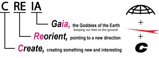
CREIA IP Attorneys
IP Law Firm in Osaka, JAPAN
Greeting

Thank you for visiting our website. CREIA IP Attorneys is an IP law firm located in Osaka, JAPAN. We provide superior services related to filing, prosecution and validation of patent, utility model, design and trademark. Please feel free to contact us regarding IP legal matters in Japan.
Our Policy
We prioritize client-oriented services with supports from various aspects of intellectual properties as well as conducting PDC (*1) to our clients. Our attorneys are capable to practice all the technical fields (e.g. electrical, mechanical, chemical, and business model field). Moreover experienced attorneys are dedicated to conduct a series of involved procedures, which will consolidate the relationship with our clients.
*1: Plan, Do, Check
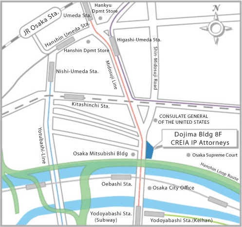
CREIA IP Attorneys
Dojima Building 8F, 2-6-8 Nishitenma, Kita-ku, Osaka 530-0047, JAPAN
TEL:+81-6-6312-0500
FAX:+81-6-6312-0501
EMAIL: creia@ダミーテキストcreia-pat.com